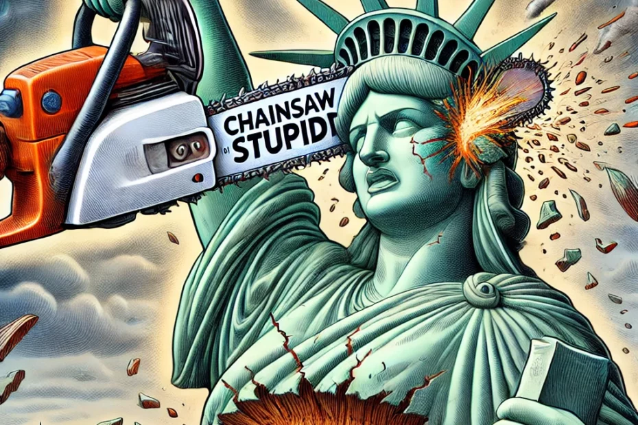
What’s Cooking at OYR (and at my house): The Chainsaw of Stupidity
Is the US still the world’s preeminent destination for the best and brightest minds in science, engineering, and technology?
Is the US still the world’s preeminent destination for the best and brightest minds in science, engineering, and technology?

The semiconductor industry must grapple with a stark new reality. The foundation upon which enterprises operate is being weakened and threatened by actions indicating the US government believes it can ignore the law and due process or make them conditional rather than guaranteed.
By Ron Wilson
What’s at stake:
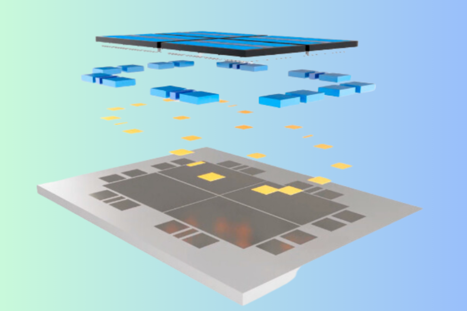
Integrated circuits operating at high speed generate a lot of heat, enough to destroy themselves and their surroundings. With the advent of dense advanced-packaging modules for AI, the old solutions are no longer sufficient, and the race is on to find alternatives. The demands are intense, however, and all players, including EDA vendors and physical analysis solutions vendors will have to team up with design engineers to develop a common thermal model with packaging companies.
Recently discussions have flared up about thermal issues in advanced packaging. But since the beginning of the semiconductor industry heat has lurked just below the surface, threatening to bubble up and make a mess of project schedules and system performance.
Today, as the inexhaustible demands of AI drive a convergence of Angstrom-era dies, advanced 3D packaging, and liquid cooling, the pot is boiling over.
Read More »The Heat is on for Multi-die Design
Anyone involved in the design of large digital silicon chips is familiar with the term Network-on-Chip (NoC), but relatively few people are cognizant of the underlying concepts.
By Ron Wilson
What’s at stake:
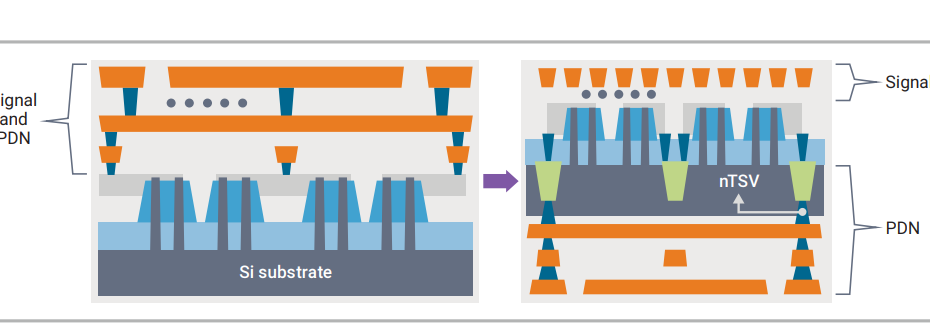
Backside Power Delivery is being promoted by all three foundry majors. It has advantages, but will substantially complicate wafer processing and multi-die module design, with undetermined costs to users. Intel, TSMC, and, more faintly, Samsung are singing the praises of backside power delivery (BPD). Recently, Synopsys raised their voice in harmony, pledging support for TSMC’s efforts. But what is BPD, what does it imply, and who, outside the giant foundry trio, really cares?
This story begins a decade ago, when foundries began drilling tiny holes deep into wafers and then thinning the wafers — grinding away the back side of the wafer until the remainder was thin enough to expose the bottom of the hole. Filled with conductive material, the hole became a via — an electrical path from the front side to the back side of the wafer. This allowed connections on the back of the wafer for easier packaging and die stacking.
Read More »Getting to the Bottom of Backside Power Delivery
By Ron Wilson
What’s at stake:
In the near future, quantum computers may be able to decrypt any data protected by public-key cryptography — effectively eliminating privacy and security from the global digital world. Can we prevent it?
There is growing discussion among the information-technology community of post-quantum, or quantum-safe, cryptography. Recently the discussion has surfaced in the semiconductor industry as well, with at least two semiconductor IP announcements: from university spin-off PQShield, and from security veteran Rambus. So what is post-quantum cryptography? Why should we care? And if we should, why now?
Read More »Will Quantum Computing Eliminate Privacy?
By Ron Wilson
What’s at stake:
Increasingly systems houses, rather than chip companies, are designing the silicon for their systems and optimizing it for their workloads. Their needs are altering the traditional chip design flow.
Two closely linked changes in the semiconductor industry are gradually altering the way ICs are designed, demanding new skills from designers, inspiring new tools from the EDA industry, and opening new roles for AI in the design flow. In a recent conversation with Synopsys VP for Product Management and System Solutions Tom De Schutter we explored this evolution.
Read More »Shift from Hardware-Defined SoCs to Workload-Optimized Chips
All that glitters is not gold. Companies must use caution in chasing targets they can’t capture or objects that are less valuable than imagined.
By Ron Wilson
What’s at stake:
With all the talk of chiplets, it is important to have a perspective on what the real issues are, and where the industry stands with them. Looking into it, we find three categories of answers.
Chiplets, systems in package, multi-die modules — there is a whole new vocabulary growing up around the old idea of putting more than one die into an IC package. By now the words, the technologies they represent, and the supply chains necessary to achieve them are resolving into three main categories, all under the general heading of multi-die modules (MDM).
The first category — well represented by recent massive GPU and datacenter CPU designs — best fits the acronym SiP. The second category — just emerging today — we might call decomposed SoCs. And the third category — arguably still several years away — we can properly call chiplet-based systems. To define each of these, we should discuss the issues that separate them and the issues they have in common.
Read More »The Chiplet Revolution: Where We Stand Today
By Ron Wilson
What’s at stake:
The leading edge of the semiconductor industry is struggling mightily to reach what they have named the Angstrom era. The phrase refers to an arbitrary point, somewhere around the so-called 3 nm process node, where it becomes fashionable to name technology nodes in Angstroms rather than in nanometers — hence, not 1.5 nm but 15 Angstroms. It is at about this point that the requirements for ever more detailed patterns on silicon wafers exceed the capabilities of today’s EUV lithography systems and procedures.
It is possible with great care nowadays to print patterns on the surface of a wafer in which the lines are about 13 nm apart — just fine enough for today’s so-called 5 nm processes. These patterns are projected onto a layer of radiation-sensitive material — a photoresist layer, so-called for mostly historical reasons. The pattern is then developed, and transferred through rather tortuous etching and cleaning processes to temporary layers of material that lie just beneath the resist. These layers, in turn, form a hard barrier through which material can be etched away, or added to the surface of the wafer to form the transistors and wires that make up the IC.
For the 3 nm generation, the most critical layers — such as those that make electrical connections to the transistors or that make up the first levels of metal interconnect — will require resolution just slightly finer than 13 nm in order to make connections to the most closely packed transistors. That is beyond the capabilities of today’s EUV systems with today’s procedures.
Read More »Tale of High-NA EUV Lithography: Two Paths Diverged