
Acute Shiny Object Syndrome Can Ruin You
All that glitters is not gold. Companies must use caution in chasing targets they can’t capture or objects that are less valuable than imagined.
All that glitters is not gold. Companies must use caution in chasing targets they can’t capture or objects that are less valuable than imagined.
By Ron Wilson
What’s at stake:
With all the talk of chiplets, it is important to have a perspective on what the real issues are, and where the industry stands with them. Looking into it, we find three categories of answers.
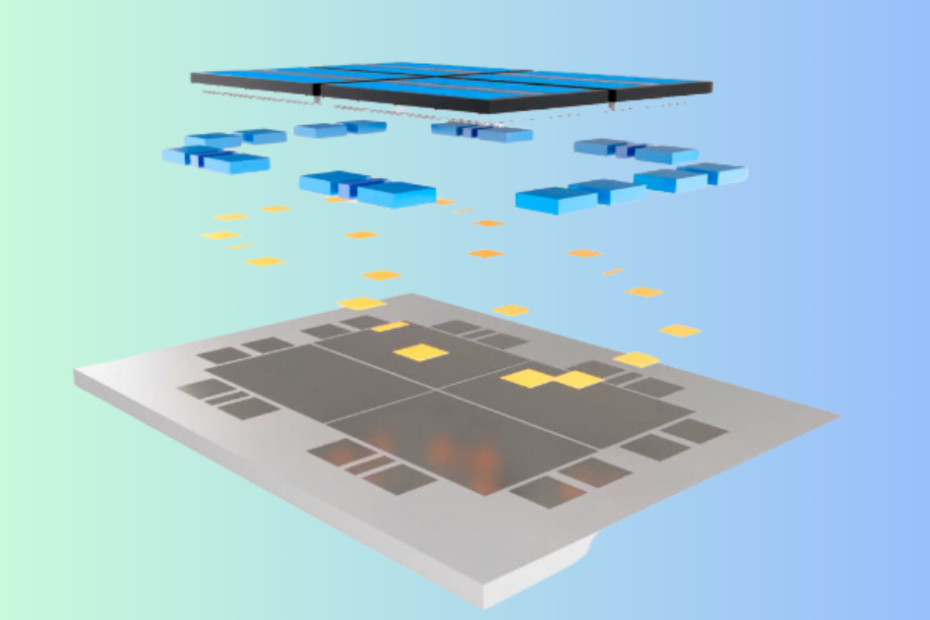
Chiplets, systems in package, multi-die modules — there is a whole new vocabulary growing up around the old idea of putting more than one die into an IC package. By now the words, the technologies they represent, and the supply chains necessary to achieve them are resolving into three main categories, all under the general heading of multi-die modules (MDM).
The first category — well represented by recent massive GPU and datacenter CPU designs — best fits the acronym SiP. The second category — just emerging today — we might call decomposed SoCs. And the third category — arguably still several years away — we can properly call chiplet-based systems. To define each of these, we should discuss the issues that separate them and the issues they have in common.
Read More »The Chiplet Revolution: Where We Stand Today
By Ron Wilson
What’s at stake:
The leading edge of the semiconductor industry is struggling mightily to reach what they have named the Angstrom era. The phrase refers to an arbitrary point, somewhere around the so-called 3 nm process node, where it becomes fashionable to name technology nodes in Angstroms rather than in nanometers — hence, not 1.5 nm but 15 Angstroms. It is at about this point that the requirements for ever more detailed patterns on silicon wafers exceed the capabilities of today’s EUV lithography systems and procedures.
It is possible with great care nowadays to print patterns on the surface of a wafer in which the lines are about 13 nm apart — just fine enough for today’s so-called 5 nm processes. These patterns are projected onto a layer of radiation-sensitive material — a photoresist layer, so-called for mostly historical reasons. The pattern is then developed, and transferred through rather tortuous etching and cleaning processes to temporary layers of material that lie just beneath the resist. These layers, in turn, form a hard barrier through which material can be etched away, or added to the surface of the wafer to form the transistors and wires that make up the IC.
For the 3 nm generation, the most critical layers — such as those that make electrical connections to the transistors or that make up the first levels of metal interconnect — will require resolution just slightly finer than 13 nm in order to make connections to the most closely packed transistors. That is beyond the capabilities of today’s EUV systems with today’s procedures.
Read More »Tale of High-NA EUV Lithography: Two Paths Diverged
By Ron Wilson
What’s at stake:
With 3nm processes barely in production, the industry is already talking about 2nm — and sliding the schedules. With a whole new kind of transistor and massive technical challenges, 2nm will be a heavy lift not only for the foundries, but for the EDA companies that have to support it and the customers who have to design for it.
Almost drowned out by the shouting about chiplets, the so-called 2nm process node — the next full step after 3nm — is moving toward production. It promised developers of CPUs, GPUs, AI chips and, eventually, smartphone application processors, a whole lot more transistors, a little less power consumption — if designers are very careful — and a lot more hard work.
But what is the reality? When is 2nm coming? How is it different from 3nm? And what has to happen to make 2nm a useable process for actual chip designers?
Read More »What’s the Story with 2nm?
By Ron Wilson
What’s at stake:
Ideally, chiplets could be off-the-shelf products that snap together like building blocks — no EDA tools required. Anyone who could specify exactly what they wanted could create a system-in-package implementation, opening up silicon to a far wider range of designers, and, incidentally, undermining parts of the EDA and design-services industries. Could it ever really happen?
One early conception of chiplets — in their formative days within the US Department of Defense — was of an open market. You could buy the functions you needed off the shelf, arrange them into a multi-die assembly, and after verification and analysis have a finished hardware design. Later thinking took this idea ever further. What if you could, figuratively speaking, just snap the chiplets together like building blocks, with no complex design automation tools or analyses needed, and could be sure that the resulting assembly would work correctly?
Read More »Can Chiplets Make SoC Design a Child’s Play?
By Ron Wilson
What’s at stake:
Arm’s public offering could be a chance to invest in the explosive growth of artificial intelligence. Or investors could be buying into a total misunderstanding of Arm and what it does — whether AI takes off or not.
No recent tech IPO has stirred as much discussion as Softbank’s plan to float about ten percent of Arm Ltd. on the US NASDAQ exchange. Although Softbank has quietly backed off from their initial suggestions about an offering price, the figures still imply earnings growth close to that of Nvidia. That is, astronomical.
Read More »Is Arm’s IPO This Year’s Best AI Play?
By Ron Wilson
What’s at stake:
What lies in the future for chiplets? They could change the structure of the semiconductor industry, freeing it from the geriatric grip of Moore’s Law and the hegemony of three giant manufacturers. Or they could, like thin-film hybrids and multidie packages before them, withdraw into a few application niches where their challenges are manageable and their costs acceptable.
By Ron Wilson
What’s at stake:
Chiplets could break through the barriers obstructing Moore’s Law and disrupt the semiconductor supply chain. But they depend on sometimes-complex packaging solutions that are far from established technologies.
With their claimed ability to deconstruct one massive, leading-edge SoC into an assembly of smaller dies built in less-aggressive processes, chiplets hint at a way forward that bypasses the dotage of Moore’s Law. By offering an alternative, they also promise a diversion around the two-party monopoly on chip fabrication beyond 10nm, suggesting more diverse, robust supply chains.
Read More »Chiplets Are Still a Work in Progress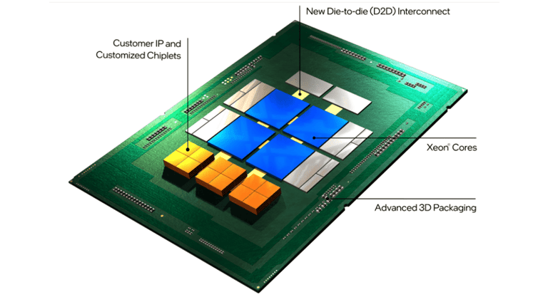
By Ron Wilson
What’s at stake?
Advanced semiconductor packaging are neither routine nor affordable. But if they were, the industry could experience the triggering of an avalanche of chiplets, allowing IP vendors to sell silicon, erase many of the advantages of rich design teams and disaggregate the IC supply chain.
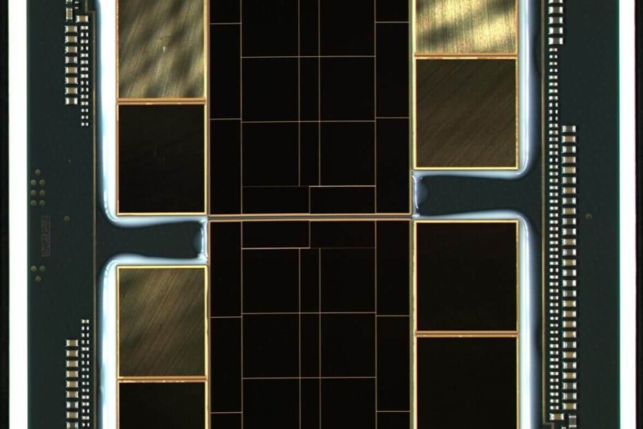
Many dies in one package. This is getting to be the topic of the month in the industry. But there are several subjects interdigitated in this area, and they are rapidly getting tangled together. This article combs them out by examining three different but related topics: multiple dies in a package; advanced packaging and; chiplets.
Read More »Advanced Packaging Holds Key to Chiplet Surge
By Ron Wilson
What’s at stake:
With all the claims and commentary about AI systems, you can’t tell the insightful from the frightful without a program. That means digging into the different things hiding under the AI umbrella.
Artificial Intelligence (AI) is everywhere. From medical research labs to your car, from police stations to your vacuum cleaner, there is no escaping it. This ubiquity begs for a good definition. But there is no simple definition — a myriad of different technologies huddle under the AI umbrella.
Unfortunately, the term itself can add perceived value to a product. So AI gets stretched beyond its natural bounds, to fit any situation where it might improve profit margins. But to understand what is really happening with AI today we need a more precise definition.
Read More »Who’s in the Zoo: A Brief Taxonomy of AI Systems