Being able to interconnect many chiplets at performance and power levels closer to those of on-die interconnect could allow design of genuinely enormous systems.

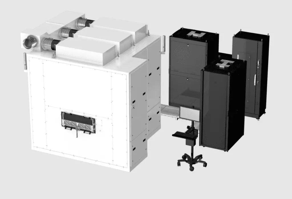
Applied Materials and Ushio are introducing a breakthrough digital lithography system for glass and other large package substrates that enables high-performance heterogeneous chip designs for the AI era of computing. (Image: Applied Materials)
By Ron Wilson
What’s at stake:
One of the most important issues — and one of the least discussed — in creating multi-die systems is the substrate technology. There are several roads into the future, going in different directions. But one of them holds unique promise.
Much of the current excitement about chiplets tends to overlook an important point. Every multi-die system-in-package rests — quite literally — on a substrate. The characteristics of that substrate influence everything about the finished system, from the architecture to the cost to the likelihood of it ever reaching customers.
