Intel is committed to a monumental struggle to catch TSMC in process technology. Will their efforts pay off?

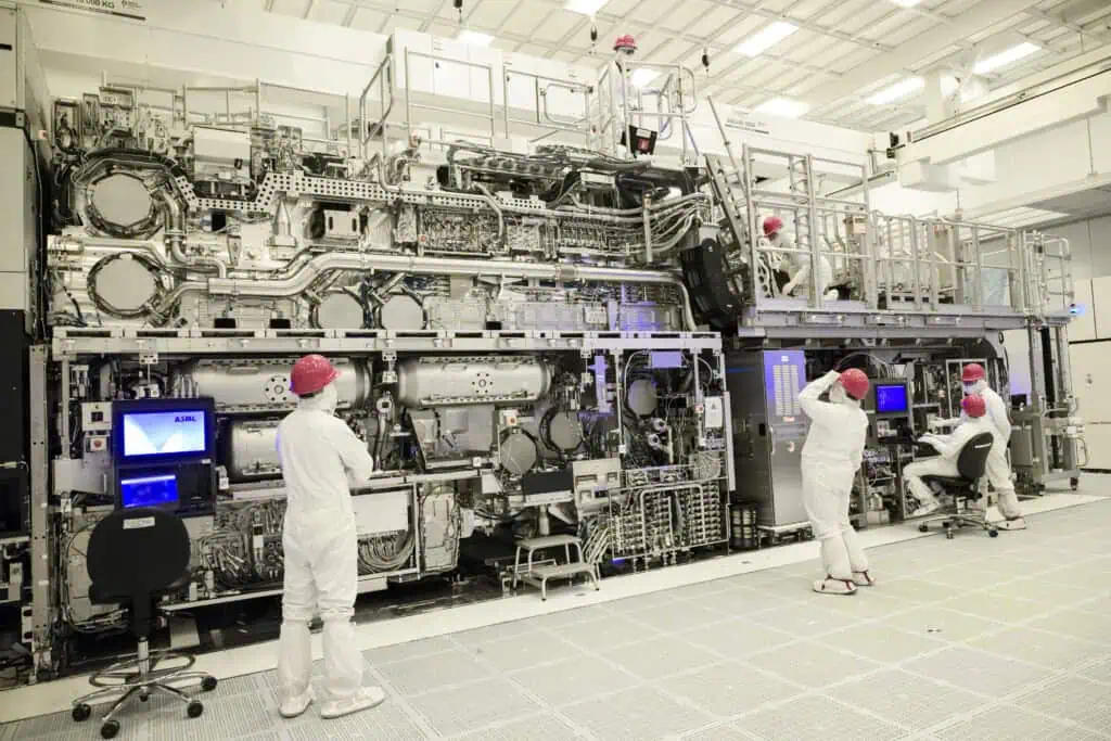
Installation is complete and calibration started on Intel's High Numerical Aperture Extreme Ultraviolet lithography tool in a clean room at Intel's Fab D1X in Hillsboro, Oregon, in April 2024. (Image: Intel Corporation)
By Ron Wilson
What’s at stake:
Intel has bet its chance to catch TSMC at the 1.4 nm node on being the first user of high-NA EUV lithography. It is a short road full of challenges, but early results look promising.
Lithography giant ASML announced this month that they have successfully printed a dense line pattern with 10 nm spacing, using the world’s first production high-NA EUV lithography system. In itself this is just another milestone in a long development schedule for ASML — similar patterns have already been printed using laboratory equipment. But in the global competition between Intel and TSMC for Angstrom-era semiconductor dominance, the announcement looms across the horizon like the first hints of dawn.
