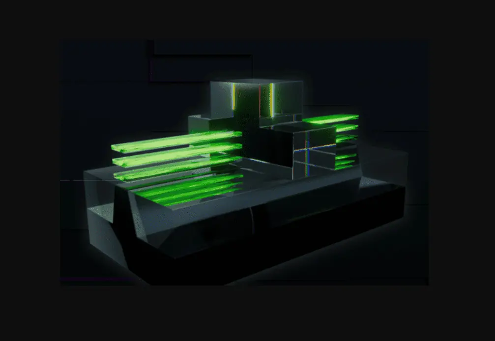
At 2 nm, a gate-all-around transistor is made up of multiple nanosheets, or ribbons--only a few atoms thick--of silicon, passing through the gate material. Here the ribbons are green, and the gate is the large black block through which the ribbons pass.
By Ron Wilson
What’s at stake:
With 3nm processes barely in production, the industry is already talking about 2nm — and sliding the schedules. With a whole new kind of transistor and massive technical challenges, 2nm will be a heavy lift not only for the foundries, but for the EDA companies that have to support it and the customers who have to design for it.
Almost drowned out by the shouting about chiplets, the so-called 2nm process node — the next full step after 3nm — is moving toward production. It promised developers of CPUs, GPUs, AI chips and, eventually, smartphone application processors, a whole lot more transistors, a little less power consumption — if designers are very careful — and a lot more hard work.
But what is the reality? When is 2nm coming? How is it different from 3nm? And what has to happen to make 2nm a useable process for actual chip designers?
